India’s semiconductor ambitions are gaining momentum as global technology leaders deepen investments to build a resilient domestic ecosystem. In a significant development, Intel, the Odisha government, and US-based 3D Glass Solutions (3DGS) have signed a $3.3-billion memorandum of understanding to expand substrate manufacturing technology in India.
The proposed facility, to be located in the Bhubaneswar-Khurda region, will be developed in phases over the next five to six years and is expected to generate over 1,800 high-skilled jobs. The investment marks one of the largest commitments in India’s high-tech manufacturing sector and reinforces the country’s positioning in the global semiconductor value chain.
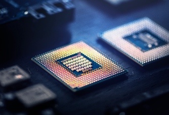
The project will focus on advanced packaging technologies, including glass core substrates and high-density interconnect (HDI) substrates, which are critical for next-generation computing systems. These substrates play a key role in enabling higher processing power, supporting complex multi-chip architectures such as AI processors, and improving efficiency by reducing electrical path lengths.
Officials highlighted that Intel will contribute significant technology expertise and process know-how, facilitating knowledge transfer and strengthening India’s semiconductor capabilities. The initiative is also expected to catalyze the development of a local supplier ecosystem, promote export-oriented manufacturing, and accelerate workforce skill development in Odisha.
The investment builds on existing momentum in the state, where 3DGS subsidiary HIPSPL is already establishing an advanced packaging and embedded glass substrate unit. The development aligns with India’s broader strategy to attract global semiconductor investments, although its inclusion under the India Semiconductor Mission 2.0 remains under consideration.
.jpg "Textile Special")



We use cookies to ensure you get the best experience on our website. Read more...