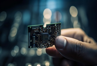
Paras Semiconductors, a subsidiary of Paras Defence and Space Technologies, has partnered with US-based BroadPak Corporation to strengthen India's semiconductor packaging capabilities.
The partnership will focus on 3D chip packaging and advanced integration technologies. The companies aim to establish an advanced outsourced semiconductor assembly and test (OSAT) facility in India.
The proposed facility will support next-generation semiconductor applications, including artificial intelligence (AI), high-performance computing, networking and data centers.
Under the partnership, Paras Semiconductors plans to develop an advanced heterogeneous integration and 3D packaging facility. The unit will focus on several emerging semiconductor technologies, including:
Paras Semiconductors will gain access to BroadPak's design, manufacturing and integration intellectual property. The agreement also covers technology transfer and process know-how.
Both companies will explore the joint development of packaging platforms for AI and high-performance computing applications. They also plan to collaborate on training Indian engineers in advanced packaging technologies.
Also Read: How Women Leaders Are Shaping India's Electric Mobility Future
Founded in 2007, BroadPak is headquartered in San Jose, California. The company specializes in advanced packaging design, manufacturing and system integration.
Munjal Sharad Shah, Managing Director of Paras Defence and Space Technologies, said the partnership represents a strategic expansion into a technology area that is becoming increasingly important for India's AI, data center and industrial capabilities.
Paras Semiconductors CEO Santosh Kumar said the company aims to build a packaging platform that addresses the performance, connectivity and thermal requirements of next-generation applications.
BroadPak Founder and CEO Farhang Yazdani highlighted India's growing semiconductor ecosystem. He said it presents an opportunity to develop local capabilities in heterogeneous integration and system-level packaging.
The proposed facility will cater to high-volume manufacturing and strategic electronics requirements. Its target applications will include:
The partnership is expected to support India's efforts to strengthen its domestic semiconductor ecosystem and develop advanced 3D chip packaging capabilities.






We use cookies to ensure you get the best experience on our website. Read more...